Detector Development
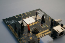
The goal of the High-Luminosity Upgrade of the LHC (HL-LHC) is to increase the instantaneous luminosity, and thus the number of collisions per time, by a factor of 10 compared to the currently achieved value. Thus, the experiments can collect significantly more data to observe rare processes. Due to the higher collision rate, many more particles per time pass through the detectors of the ATLAS experiment, resulting in particularly high demands on the technology, especially of the innermost components, the inner track detector (Inner TracKer, ITk). The detectors must be very fast, made of as little material as possible, and have very good spatial resolution. As part of the ITk detector upgrade, we are working on tests of the novel pixel detectors, in particular using so-called test beam studies, and are actively involved in the construction of detector modules for the strip detector. The new detector is expected to begin operation in 2027.
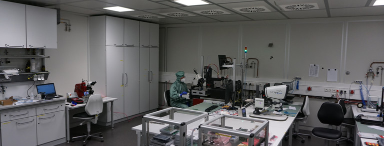
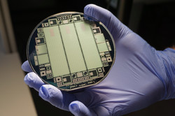
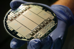
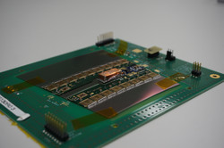
In addition to the requirements for hit rate, radiation hardness, spatial resolution, and hit efficiency, the large area that must be instrumented in modern particle physics detectors presents an enormous challenge. All processes in the construction of such detectors must be increasingly industrialized in order to be able to produce sufficiently large quantities of detector modules. As a result, large manufacturers of CMOS imaging sensors are becoming more involved in production, as their factories are geared towards enormously high volumes. To take advantage of this resource, detector physicists are intensively exploring the possibilities of CMOS fabrication of charged particle detectors. Our activities are focused on two different areas. On the one hand, we examine passive stripe sensors, which were manufactured in a CMOS factory. These sensors are connected to known readout chips to characterize them by electrical tests in the laboratory and by test beam measurements. The advantage of this approach is that the large strip sensors can be manufactured particularly cost-effectively. The second approach is the production of active pixel detectors, where the readout electronics are built right into the sensor. This allows the low-cost sensors to be made significantly thinner at the same time, which has great advantages especially for the innermost detector layers.
Furthermore, we are engaged in the development of ultra-fast silicon detectors (UFSD), which achieve a time resolution on the order of a few tens of picoseconds on the basis of avalanche diodes. This type of detector can be used in high-energy physics experiments to assign particles to the correct interaction in areas with very high track densities.
Funded by:
- DFG INST 212/463-1 FUGG (Semi-automatic wafer prober)
- BMBF 05H21PERD1
- BMBF 05H21PECA9


